12th Annual IEEE 1999 International
ASIC/SOC Conference,
Washington DC, USA, 15-18 September 1999
© Copyright 1999 IEEE
ATLAS I (ATm multi-LAne backpressure Switch One) is a high performance, single chip ATM switch designed in (the Computer Architecture and VLSI Systems Division, of the Institute of Computer Science of) FORTH, Crete, Greece, to provide a powerful, yet cost effective building block for the creation of ATM networks [1, 2, 3]. ATLAS I combines several features that are desirable for building such networks:
In this paper we attack the problem of overall efficiency of the ATLAS ATM switch and we show that relatively minor changes in the functionality and in the implementation circuitry can have a significant impact on the overall area of the switch (i.e. on its cost), as well as on the cut-through latency of cells through the switch (i.e. on its performance). The rest of this paper is structured as follows: In section 2 we briefly describe the main features of ATLAS I. Next, in section 3, we describe a re-design of ATLAS I, and we show how much more compact the chip could be made, while maintaining the same logic and functionality. In section 4 we describe ATLAS II, an improved version of ATLAS I; here we attack the problem of overall efficiency, we allow changes in the functionality, and we remove features that are not worth their cost (as described in [3]). Finally, we present our conclusions in section 5.
ATLAS I is a 6 million transistor chip designed in a 0.35 micron CMOS technology with five metal layers provided by ST Microelectronics. It features 16 input and 16 output ports (links) each operating at 622Mbits/s [4] for an aggregate outgoing throughput of 10Gbits/s; the links use the IEEE 1355 ``HIC/HS'' protocol [5]. The switch core operates at 50 MHz and achieves a sub-microsecond cell cut-through latency. Buffer space for the ATM cells is provided in the form of a 256-cell (entry) shared buffer, partitioned into multiple logical output queues; ATLAS I also supports three levels of priorities, multicasting and header translation.
The most distinctive and innovative feature of ATLAS I is its (optional) credit-based flow control (backpressure). A cell in a backpressured service class (priority level) can only depart if it acquires both a buffer-pool credit for its outgoing link and a flow-group credit for its connection. A flow group is a set of connections that are flow-controlled together; ATLAS I supports up to 2 thousand flow groups per outgoing link. Switching fabrics built with internal backpressure combine the high performance of output queuing with the low cost of input buffering; additionally, these fabrics never drop cells of data connections, while they fully and fairly utilize all the available transmission capacity. An evaluation performed at FORTH shows that the credit protocol offers superior performance, especially in isolating well-behaved connections from bursty and hot-spot traffic [6]. The advantages of the credit-based flow control have also been underlined by other researchers [7, 8] and products [9].
ATLAS I also provides for efficient network load monitoring by means of accelerated Cell Loss Probability (CLP) measurement hardware. Very often in high-speed networks the probability of cell loss (for non-backpressured traffic) is so small that measuring it requires a very long observation period. The ATLAS I CLP hardware measures the cell loss rate of an emulated set of small buffers. Software can then use these measurements (over short periods of time) to extrapolate the CLP of the actual traffic [10]. ATLAS I also provides hooks for switch management through the network: special management cells addressed to an internal management port, can execute read and write commands to any of the internal structures of the switch. The results of these operations are packed in a reply cell and returned to the sender. More details on the architecture of ATLAS I can be found at http://archvlsi.ics.forth.gr/atlasI.
In this section we present how efficient the implementation of ATLAS I would have been, had we concentrated on area reduction rather than on prototyping speed and ease of implementation. The area that is absolutely necessary depends on several factors but can be roughly categorized into: (i) storage for cells, routing tables and credits, (ii) logic for interfacing the transceivers to the switch core, and (iii) logic that implements the crossbar switch and manages the entire chip. These abstract categories apply to all switches that provide functionality similar to the one offered by ATLAS I, and the cost estimates we present here can be easily used to extrapolate the cost of a switch similar to ATLAS I.
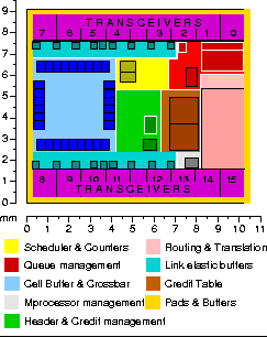
Figure 1: ATLAS I floorplan: (a) as was fabricated on January 1999, and (b) compacted for minimal area.
Starting with this first implementation, we need to remove all the design
waste and produce a compacted implementation of ATLAS I, so we can obtain
a meaningful base for comparisons. We achieved this by compacting both
the high speed serial transceivers and the switch core. In the core of
the switch we removed the block boundaries that are visible in Figure 1(a).
The resulting new floorplan for ATLAS I is shown in Figure 1(b);
the dimensions are now ![]() , a significant improvement in the die size (47%). The standard cell area
utilization is set to a comfortable 80% which, according to our experience,
is low enough to produce satisfactory results with few place and route
iterations.
, a significant improvement in the die size (47%). The standard cell area
utilization is set to a comfortable 80% which, according to our experience,
is low enough to produce satisfactory results with few place and route
iterations.
The compacted implementation of ATLAS I is identical to the original one in every respect, except one: the total number of pads. In ATLAS I, the unused east and west side pads were used to implement a microprocessor interface, and four low-speed parallel interfaces for test purposes. In the new area-effective implementation the perimeter and hence the number of pads is smaller so we had to reduce the number of the parallel interfaces down to two, retaining some of the ability to perform low speed testing, while reducing the overall number of pads.
Summarizing, we used a very simple compacting methodology in order to achieve an area-effective implementation of ATLAS I; in the rest of this paper we will use this implementation as the base for area comparisons.
To further optimize the implementation cost and the performance of he switch we need to utilize better (more efficient) circuitry, and modify the functionality provided by the switch. First we concentrate on the circuitry.
Another large area penalty in ATLAS I is the CAM used to match incoming
cell headers to the appropriate parameters for their handling. This is
a 40 entry 37-bit CAM that drives a ![]() bit memory. In ATLAS I this was implemented with semi-custom logic and
required a total area of
bit memory. In ATLAS I this was implemented with semi-custom logic and
required a total area of ![]() . For a quick comparison, the ATLAS I implementation contains a
. For a quick comparison, the ATLAS I implementation contains a ![]() -bit CAM designed in full custom VLSI that occupied only
-bit CAM designed in full custom VLSI that occupied only ![]() [12]. It is clear that the area efficiency
of the semi-custom CAM is very low, so for ATLAS II we designed the header
matching CAM in full-custom VLSI. This full-custom CAM implements the same
functionality and interface, but requires only
[12]. It is clear that the area efficiency
of the semi-custom CAM is very low, so for ATLAS II we designed the header
matching CAM in full-custom VLSI. This full-custom CAM implements the same
functionality and interface, but requires only ![]() , corresponding to an area reduction of 86 %. Furthermore, the operating
speed of the full-custom CAM is 2 times larger than the semi-custom one.
, corresponding to an area reduction of 86 %. Furthermore, the operating
speed of the full-custom CAM is 2 times larger than the semi-custom one.
The third and final space optimization is in the interfaces that connect the switch core to the high-speed serial links. Each of the 16 interfaces contains a 256-entry memory that stores credits until they can be transmitted. The need for this memory arises from the restriction that at each cell time (33 cycles) at most two credits can be transmitted to the link (to keep down the required rate of handling incoming credits at neighbor ATLAS switches), but up to 16 credits can be generated inside the core. Despite the fact that the steady-state rate is only one credit per cell time, in the worst case up to 256 credit can accumulate in the credit queue of a link; the value 256 is determined by the size of the cell buffer, since each departing cell may generate a credit. However, this worst case scenario can only happen for one of the output interfaces, while all of them contain 256-entry memories. We can reduce the required area by providing smaller individual queues for each link and maintain an overflow queue that will be used when the smaller queues fill-up [13]. In ATLAS II we opted for a 128-entry queue per I/O link interface, with a centralized overflow queue of 128 entries.
Putting together all the optimizations we described in this section,
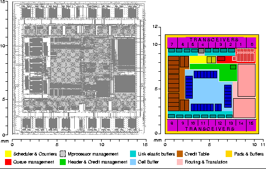
we arrived at the final floorplan for the ATLAS II switch shown in Figure
2.
The dimensions of the die are ![]() , giving an improvement of 20% of the die area compared to the compacted
implementation of ATLAS I.
, giving an improvement of 20% of the die area compared to the compacted
implementation of ATLAS I.
In ATLAS I, cell processing begins as soon as the cell data are received and are transferred in parallel from the transceivers to the switch core. These data are clocked with a recovered clock and must be synchronized with a different clock before we can use them in the core. Next comes a small elastic buffer, required to guarantee uninterrupted delivery of the cell (an implicit assumption in our implementation) in face of possible transmission frequency variations between chips. After the elastic buffer, the cell data are sent to data buffers, while the header is presented to the header processing pipeline which contains three major functions: header serializing, matching headers to the corresponding processing parameters, and the actual header processing (routing table access, possible header translation, credit handling, etc). After this processing the cell is ready to be inserted in the appropriate queues and be stored into the cell buffer. Assuming the cell can be scheduled for departure immediately, the scheduler will notice the availability of a cell in a queue and schedule the cell for transmission, informing the cell buffer to begin fetching the data of the cell. The data are then presented to the output elastic buffer, and from there they are sent to the serial transceiver. The first column of Table 1 presents the break-down of the ATLAS I cell cut-though latency according to the individual functions.
Most of the types of the described latencies are inherent to the overall structures of the switch. For example, synchronizing the incoming cell data is unavoidable; similarly, the headers must be serialized and the routing table must be consulted before we can transmit the cell to the correct output port. The individual latencies of these functions however, depend on the exact assumptions and design choices. In ATLAS I, we conservatively allowed two cycles for header serializing, another 2 cycles for the CAM based parameter mapping and three cycles for the actual header processing. Here we use three distinct tools to reduce this latency. First, by exploiting the complete duration of a cycle we can reduce the header serializing latency to a single cycle. Second, the full-custom VLSI CAM in addition to being smaller is also much faster, reducing the latency for the parameter matching to a single cycle. Third, as described earlier, in ATLAS II we removed the table-based header translation functionality; a fortunate side-effect of this change is that it removes a dependency from header processing. Intuitively, we can think of header processing as the following sequence: generate routing and translation address, access table for new header, compute parameters (credits, etc) for new header. Removing the table access for the new header allowed us to use only two pipeline stages for header processing.
One important latency reduction technique is to process the incoming
headers in parallel with the (data-related) elastic buffering. That is,
we can bypass the input elastic buffer and feed incoming headers directly
into the header processing pipeline reducing in this way the observed latency
for headers; the longer observed latency for the data of the cell will
then be hidden by header processing latency. This improvement saves a total
of six cycles (three in the elastic buffering and another three in the
header processing, but requires extra paths to drive the 40-bit header
from each input port to the header serializer (in ATLAS I we "eavesdrop"
the 16-bit cell data on their way to the cell buffer to obtain a copy of
the header). One final reduction in latency can be achieved in the cell
buffer and crossbar of the switch: since each bank of the cell memories
is small ( ![]() bits), their access time is also small. We exploit this fact and merge
the two distinct pipeline stages of memory read and crossbar operation
into a single one, reducing the cell buffering latency from 3 to 2 cycles.
bits), their access time is also small. We exploit this fact and merge
the two distinct pipeline stages of memory read and crossbar operation
into a single one, reducing the cell buffering latency from 3 to 2 cycles.
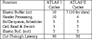
Table 1: Cut-Through Latencies for ATLAS I and ATLAS II.
The final cut-through latency breakdown is shown in the second columns of table 1. In ATLAS II the total latency is 20 cycles compared to 30 for ATLAS I, corresponding to an improvement of 33%. Observing Table 1, we can see that the bulk of the latency is in the elastic buffering, which is unavoidable considering the +-10% frequency tolerance of the switch. Conceivably, one could attempt to shortcut the queue handling to remove one or perhaps two more cycles from the dependence path. However, this optimization can be successful only if the output part of the switch is idle, i.e. it is not useful when the switch operates at full bandwidth. We believe that the benefits of this optimization are limited.
ATLAS I is an aggressive single chip ATM switch, and a powerful building block for the construction of ATM networks. In this paper we described ATLAS II, an improved implementation of ATLAS I that achieves the same throughput, using about 20% smaller die area compared to an area efficient implementation of ATLAS I and 55% smaller compared to the original ATLAS I prototype. The economized area can either reduce the chip cost, or can be devoted to other functions, such as a larger cell buffer. In addition, ATLAS II also reduces the cut-through latency by 30% from 30 to 20 cycles, improving the performance of the switch in latency-aware environments such as multicomputer networks, or networks for clusters of workstations, etc. The effort required to achieve these benefits is reasonable, since we are based on a systematic identification and solution of each of the few important design bottlenecks; these same reasons make this methodology a general one. We estimate that the ATLAS II implementation would add less than 6 man-months to the 15 man-years required for the ATLAS I implementation, while a simple re-implementation of ATLAS I would add around 2 man-months to it, and we believe that the benefits clearly outweigh the required effort.
This document was generated using the LaTeX2HTML translator Version 96.1 (Feb 5, 1996) Copyright © 1993, 1994, 1995, 1996, Nikos Drakos, Computer Based Learning Unit, University of Leeds.
The translation was initiated by Giorgos Kornaros on Mon Jul 5 11:30:27
EET DST 1999